(China (Mainland))

Product Summary
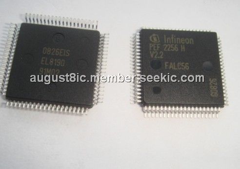
The PEF2256HV2.2 is a framer and line interface component. The PEF2256HV2.2 is designed to fulfill all required interfacing between analog E1/T1/J1 lines and the digital PCM system highway, H.100/H.110 or H-MVIP bus for world market telecommunication systems. Due to its multitude of implemented functions, the PEF2256HV2.2 fits to a wide range of networking applications and fulfills the according international standards. Three integrated signaling controllers including Signaling System #7 (SS7) support reduces software overhead. Crystal-less jitter attenuation with only one master clock source, integrated receive line termination, and an analog switch reduce the amount of required external components. Equipped with a flexible microprocessor interface, it connects to any control processor environment. A standard boundary scan interface is provided to support board level testing. Flat pack or BGA device packaging, minimum number of external components and low power consumption lead to reduced overall system costs.
Parametrics
PEF2256HV2.2 absolute maximum ratings: (1)Ambient temperature under bias TA: -40 to +85 °C; (2)Storage temperature TSTG: -65 to +125 °C; (3)Moisture Level 3 temperature TML3: +225 °C; (4)Supply voltage VDD : -0.5 to 4.50 V; (5)Supply voltage (core, digital)VDDC -0.5 to 2.40 V; (6)Supply voltage (PLL, analog)VDDP -0.5 to 4.50 V; (7)Supply voltage (receiver, analog)VDDR -0.5 to 4.50 V; (8)Supply voltage (transmitter, analog)VDDX: -0.5 to 4.50 V; (9)Receiver input signal VRLmax: -0.8 to 4.50 V; (10)Voltage on any pin Vmax: -0.5 to 4.50 V.
Features
PEF2256HV2.2 features: (1)High-density, generic interface for all E1/T1/J1 applications; (2)Analog receive and transmit circuits for long-haul and short-haul applications; (3)E1 or T1/J1 mode selectable; (4)Data and clock recovery using an integrated digital phase-locked loop; (5)Maximum line attenuation up to -43 dB at 1024 kHz (E1)and up to -36 dB at 772 kHz (T1/J1); (6)Programmable receive equalizer characteristic; (7)Software-selectable receive line termination; (8)Programmable transmit pulse shapes for E1 and T1/J1 pulse masks; (9)Programmable line build-out for CSU signals according to ANSI T1. 403 and FCC68: 0dB, -7.5 dB, -15 dB, -22.5 dB (T1/J1); (10)Low transmitter output impedances for high transmit return loss; (11)Tristate function of the analog transmit line outputs; (12)Analog switch for redundancy applications; (13)Transmit line monitor protecting the device from damage; (14)Receive line monitor mode; (15)Jitter specifications of ITU-T I.431, G.703, G.736 (E1), G.823 (E1)and AT&T TR62411 (T1/J1)are met; (16)Crystal-less wander and jitter attenuation/compensation.
Diagrams

| Image | Part No | Mfg | Description |  |
Pricing (USD) |
Quantity | ||||
|---|---|---|---|---|---|---|---|---|---|---|
 |
 PEF2256HV2.2 |
Infineon Technologies |
Network Controller & Processor ICs T/E |
Data Sheet |
Negotiable |
|
||||
| Image | Part No | Mfg | Description | |
Pricing (USD) |
Quantity | ||||
|
PEF20064EV1.2-G |
Infineon Technologies |
Network Controller & Processor ICs T/E |
Data Sheet |
Negotiable |
|
||||
|
PEF2015 |
Other |
|
Data Sheet |
Negotiable |
|
||||
|
PEF2023 |
Other |
|
Data Sheet |
Negotiable |
|
||||
|
PEF20256EV3.2-G |
Infineon Technologies |
Network Controller & Processor ICs T/E |
Data Sheet |
Negotiable |
|
||||
|
PEF2026T-PV1.1 |
Infineon Technologies |
Network Controller & Processor ICs ISDN |
Data Sheet |
Negotiable |
|
||||
|
PEF2026T-SV1.1 |
Infineon Technologies |
Network Controller & Processor ICs ISDN High Voltage Power Controller |
Data Sheet |
Negotiable |
|
||||