(China (Mainland))

Product Summary
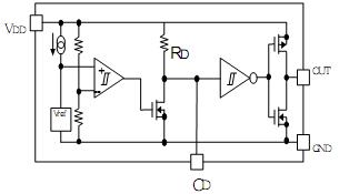
The R3112N271C-TR-F is a voltage detector ICs with high detector threshold accuracy and ultra-low supply current by CMOS process, which can be operated at an extremely low voltage and is used for system reset as an example. The R3112N271C-TR-F consists of a voltage reference unit, a comparator, resistor net for detector threshold setting, an output driver, a hysteresis circuit, and an output delay circuit. Applications of the R3112N271C-TR-F include: PU and Logic Circuit Reset, Battery Checker, Window Comparator, Wave Shaping Circuit, Battery Back-up Circuit and Power Failure Detector.
Parametrics
R3112N271C-TR-F absolute maximum ratings: (1) Output voltage VDD: 6.5V; (2) Output Voltage(CMOS) VOUT1: Vss -0.3 V-VDD +0.3V; (3) Output Voltage (Nch) VOUT2: VSS -0.3 to 6.5V; (4) Output Current IOUT: 20mA; (5) Power Dissipation PD: 250mW; (6) Operating Temperature Range Topt: -40 to 85°C; (7) Storage Temperature Range Tstg: -55 to 125°C; (8) Lead temperature (Soldering) Tsolder: 260°C, 10s.
Features
R3112N271C-TR-F features: (1) Built-in Output Delay Circuit: TYP. 100ms with an external capacitor: 0.022μF; (2) Ultra-low Supply Current: TYP. 1.0μA (VDD=3.5V) ; (3) Wide Range of Operating Voltage: 0.7 6.0V(Topt=25°C) ; (4) Detector Threshold: Stepwise setting with a step of 0.1V in the range of 0.9V to 5.0V is possible; (5) High Accuracy Detector Threshold: ±2%; (6) Low Temperature-Drift Coefficient of Detector Threshold: TYP. ±100ppm/°C; (7) Two Output Types: Nch Open Drain and CMOS; (8) Two Types of Packages: SOT-23-5 (Mini-mold) , SC-82AB.
Diagrams
 |
 R3112 |
Other |
|
Data Sheet |
Negotiable |
|
||||
|
R3111 |
Other |
|
Data Sheet |
Negotiable |
|
||||